As the semiconductor industry advances towards smaller and more complex designs and processes, electron microscopes and other advanced imaging techniques are now essential for quality control, defect detection, metrology and failure analysis. But limitations in speed cause bottlenecks, making the need for faster imaging and analysis a priority.
Firstly, the scanning speeds of imaging equipment during inline processes constrains throughput of the production line whether it’s validating the wafers, the intermediate steps such as lithography and etching or finishing the final devices. CD-SEM, TEM, SIMS and X-rays are all affected.
In nearline processes such as failure analysis, typically SEM, TEM, FIB, SAM and other analytical techniques such as EDS, EELS and EBSD, the speeds to inspect, identify and resolve root causes limits yield.
Finally, speeding up R&D, which now includes 2D-STEM and 4D-STEM, can shorten development cycles, reduce risk and increase yields.
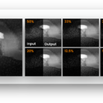
SenseAI’s compressed sensing for Electron Microscopy generates high-quality images from only a fraction of the original pixels – typically 10% but down to 1% in some cases. Because it’s scanning up to 99% less data, it’s significantly faster. This is important as more and more imaging is brought into in-line and at-line quality assurance.
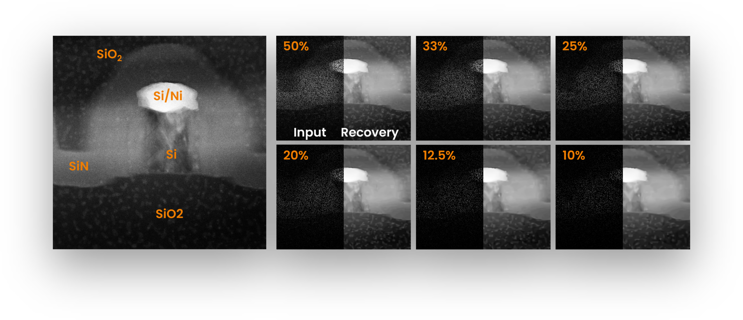
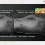
Above you can see a semicon USB being sampled at various speeds using SenseAI
The technology is based on proven mathematical algorithms which ensure that all the original information is present and therefore doesn’t require training. This compares to other forms of AI which do require training and can hallucinate, creating artefacts that aren’t there and missing ones that are. The improvements in scanning speed can be applied to all electron microscopy techniques.
And speed isn’t the only benefit. Beam damage is a big issue in semicon. In production, CD-SEMs damage the product they’re looking at due to photo-resistivity. And by using low currents, signal-to-noise then becomes an issue. Beam damage is even more acute in R&D which can alter and damage the material being characterised, meaning that the scientific analyses in inherently compromised. SenseAI uses up to 90% less beam dose meaning samples always retain their integrity. It can also impact other workflows like reducing the requirement for gold coating in some cases with reductions in charging, and reducing vacuum time for others by its benefits in denoising.
SenseAI has also unearthed another world-first for semicon – live 4D-STEM experiments. 4D-STEM images atomic resolution and measures the strains and electric field properties of a sample. Until now it’s been expensive, slow and challenging to use but now the industry can perform analysis in real time.
SenseAI’s software is compatible with all leading hardware such as JEOL, Thermo Fisher, Hitachi and Zeiss. Installation takes a matter of hours and it can run locally and securely on a standard PC.
The CNR Institute for Microelectronics and Microsystems (CNR-IMM), one of Europe’s leading semiconductor research labs, is using SenseAI to achieve a faster alignment with a lower electron dose, using just 10% of the original data.
Giuseppe Nicotra, Head of Sub-Ångstrom Electron Microscope LAB at CNR-IMM says: “In the semiconductor industry many specimens are very beam-sensitive. With SenseAI we can work at previously unachievably low doses to preserve sample integrity and benefit from superior data.
“We can perform analysis across SEM, 2D and 4D-STEM in real time. There’s nothing worse when you acquire a 4D-STEM data set and then you’re unable to know how good it is until you’ve processed and analysed it, and ten have to re-acquire the datasets. This is a lengthy process consuming huge amounts of data. With SenseAI you can see 4D-STEM images live and make adjustments on the fly.”