


Overview
Electron microscopy is a key step in any semiconductor workflow. We can use SEM (scanning electron microscopy) to analyse the bulk composition of our samples. This could look for large scale defects, and then use STEM (scanning transmission electron microscopy) for chemical and atomic analysis of those defects.
The CNR Institute for Microelectronics and Microsystems develops cutting-edge processes and technologies to create micro through nano-devices and electronic- and photonic-sensors for applications in numerous sectors, additional to the semiconductor industry.
Structural and electrical diagnostic techniques have always played a crucial role in the research activity of IMM. Our laboratory is well-known as a European centre of excellence in the development and use of electron-, ion- and X-ray characterisation techniques.
STEM and low-energy SEM enables research in the structural characterisation of materials, supporting electron crystallography, dopant profiling and often require customised imaging method development. Additionally, the laboratory is equipped to perform cryogenic TEM measurements on radiation sensitive materials such as graphene or polymers.
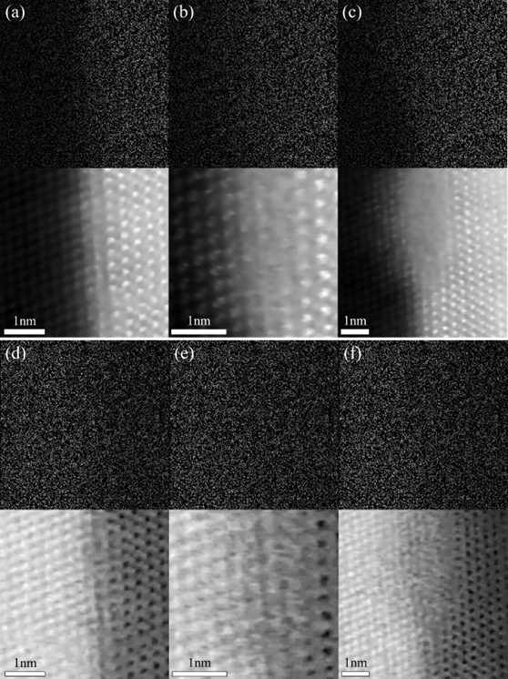
This image show live capture and inpainting of sub-sampled 4-D STEM data of an interface between silicon and germanium telluride. In this live acquisition, we simultaneously image the LAADF (a-c) and ABF (d-e) signals and inpaint them on-the-fly. We start with a pristine boundary (a, d) acquired at 200s after finding the region and correcting low-order aberrations, then increase the magnification to induce beam damage at the interface (b, e). This causes the interface to breakdown and for tellurium to diffuse across the boundary. The final damaged section can be seen after demagnifying (c, f). Data acquired at CNR-IMM, Catania, Italy. Sample provided by CNR-IMM, Catania, Italy.
Solution
- able to subsample using just 10% of the original data
- able to image in real time
- data more manageable and cost efficient
- able to preserve sample integrity
Giuseppe Nicotra, Head of Sub-Ångstrom Electron Microscope LAB at CNR-IMM talks about how they used SenseAI for their subsampling experiments.
I was really impressed with the speed of the reconstruction that SenseAI software delivers, and running it provides great economies.
Giuseppe Nicotra, Head of Sub-Ångstrom Electron Microscope LAB at CNR-IMM
For the microscope operator, it's really important to have a very reactive system, especially when you are tuning imaging parameters - you need very fast feedback. Tuning imaging parameters with SenseAI was great, and I was impressed at how SenseAI denoises, refines and reconstructs very noisy images.
In the semiconductor industry sample imaging is highly specific to the nature of the specimen, and many are very beam-sensitive. With SenseAI we can actually achieve a faster alignment with a lower electron dose. Being able to work at previously unachievably low doses, we are able to preserve sample integrity and benefit from superior data.
We can perform lots of different analysis methods using SenseAI across SEM, 2D and 4D S/TEM together with diffraction patterns and ptychography. With the ability to capture multiple different images within the same acquisition, we can also make alignment adjustments at a very high resolution.
Using SenseAI, we can rapidly test different parameters to get the maximum output from our analysis reliably. This is crucial for our laboratory.
With SenseAI we are also able to image in real time. There's nothing worse than when you acquire a 4D STEM data set and then you're unable to know how good it is until you've gone away, processed and analysed it, and have to re-acquire the datasets.
Currently EM datasets are huge, resulting in data storage management issues. Even generating these large datasets requires very long acquisition times. In our experiments using SenseAI, we are able to subsample using just 10% of the original data. We can therefore acquire very high quality data within a very small file (which can be sent within an e-mail). Maintaining large data volumes in a data centre is costly but we can now preserve and easily handle all of the required information using a lot less storage.
Key Outcomes
Data lies at the heart of neural networks, and our services start with understanding your unique data landscape. We work closely with you to identify and collect relevant data sources, ensuring that your neural network models are built on a solid foundation. Our data scientists employ cutting-edge techniques to preprocess and clean the data, making it ready for training the neural network models.
- Pacific hake false trevally queen parrotfish black
- Prickleback moss revally queen parrotfish black
- Queen parrotfish black prickleback moss pacific
- Hake false trevally queen
production